Electro-Optics Laboratory (EOL)
EOL
Electro-Optics Laboratory
Mission:
The Electro-Optics Lab was established in 1431 H (2010) with an aim to engage in design, manufacturing and testing infrared and electro-optical sensors, focal plane arrays and camera systems. The lab also aims to educate a new generation of engineers, in the above named technologies who will be the driving force for technological advancement and innovation in the Kingdom of Saudi Arabia.
Description:
Focus Areas:
In the Electro-Optics Laboratory we perform in-house design, simulation, fabrication, and characterization for our devices and systems.
The research and development activities of Electro-Optics lab are currently focused in the following areas:
- Microbolometers for infrared and millimeter wave detection.
- Infrared and millimeter wave antennas.
- Infrared and millimeter wave sensor materials.
- Metal-insulator metal diodes.
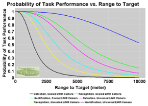
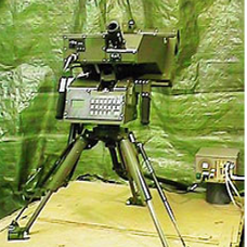
- Infrared and electro-optical imager testing.
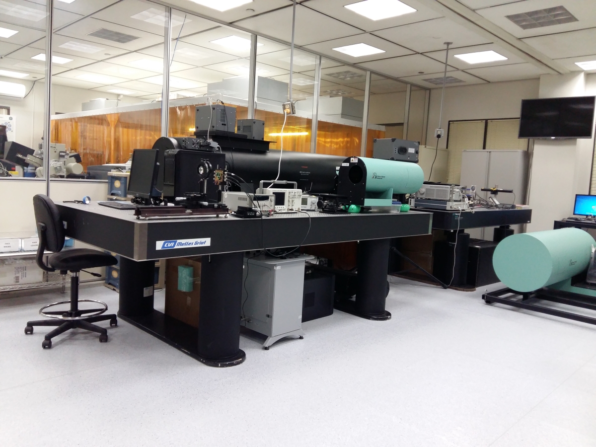
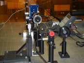
Facilities and Equipments:
 Our facilities include:
- Simulation software
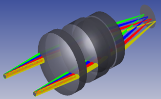
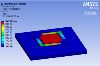
- COVENTOR for MEMS simulation.
- HFSS for antenna simulation.
- Electronics
- Agilent 35670A signal analyzer (122 µHz - 102.4 kHz).
- Ametek 5210 lock-in amplifier.
- An assortment of electronic lab equipment (DC power supplies, function generators, DMM, etc.).

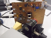
 Custom-built electronics: We build in-house custom low noise circuits for sensor bias and readout.
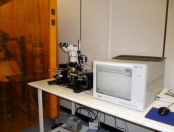
- Semiconductor Characterization
- Agilent B1500 semiconductor parameter analyzer with I-V and C-V measurement capabilities.

- Cascade Microtec EP6 DC parametric probe station.
- Vecco Dektak 150 surface profilometer for thin film profile measurements.
- JANDEL multiHeight four point probe.
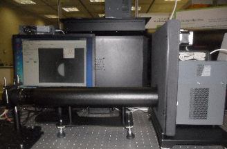
- Sentech infrared spectroscopic ellipsometer.
- Agilent B1500 semiconductor parameter analyzer with I-V and C-V measurement capabilities.
- Micro/nano Fabrication
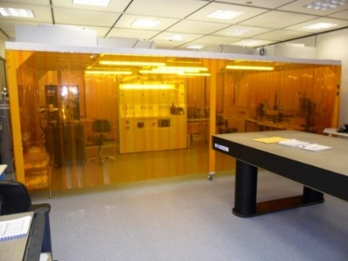
- A 22 m^2 softwall clean 1000 cleanroom.
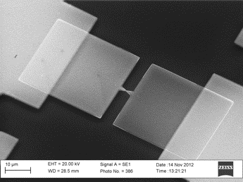
 Zeiss Scanning electron microscope (SEM) with Raith Elphy Quantum nanolithography module for electron-beam lithography.
- NXQ 4004 contact mask aligner for photolithography.
- AJA International magnetron sputtering system for deposition of thin metallic and non-metallic films.
- Diener Electronics reactive ion etcher and plasma asher.
- FELCON fume hood with BOE etch bath.
- Olympus MX51 semiconductor inspection microscope.
 Hybond ultrasonic Wire Bonder.
- ATV RV129 manual wafer scriber.
- Brewer Science CEE 200 spin coater.
- Brewer Science C1300 hot plate.